-
Sep 7, 2026, 10:00 pm246 ptsTop Tom's Hardware
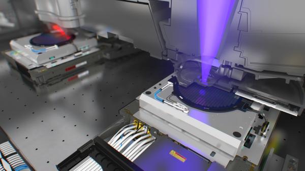 Intel announced on Monday that it had processed more than one million 300-mm wafers using its High-NA EUV scanners, less than two and a half years after its first tool was assembled. For now, the company intends to use industry-standard 6-inch photomasks, which can expose 26×16.5 mm half-fields and therefore…
Trending Today on Tech News Tube













Tech News Tube is a real time news feed of the latest technology news headlines.
Follow all of the top tech sites in one place, on the web or your mobile device.
Follow all of the top tech sites in one place, on the web or your mobile device.